The job listing no longer exists.
Open Positions
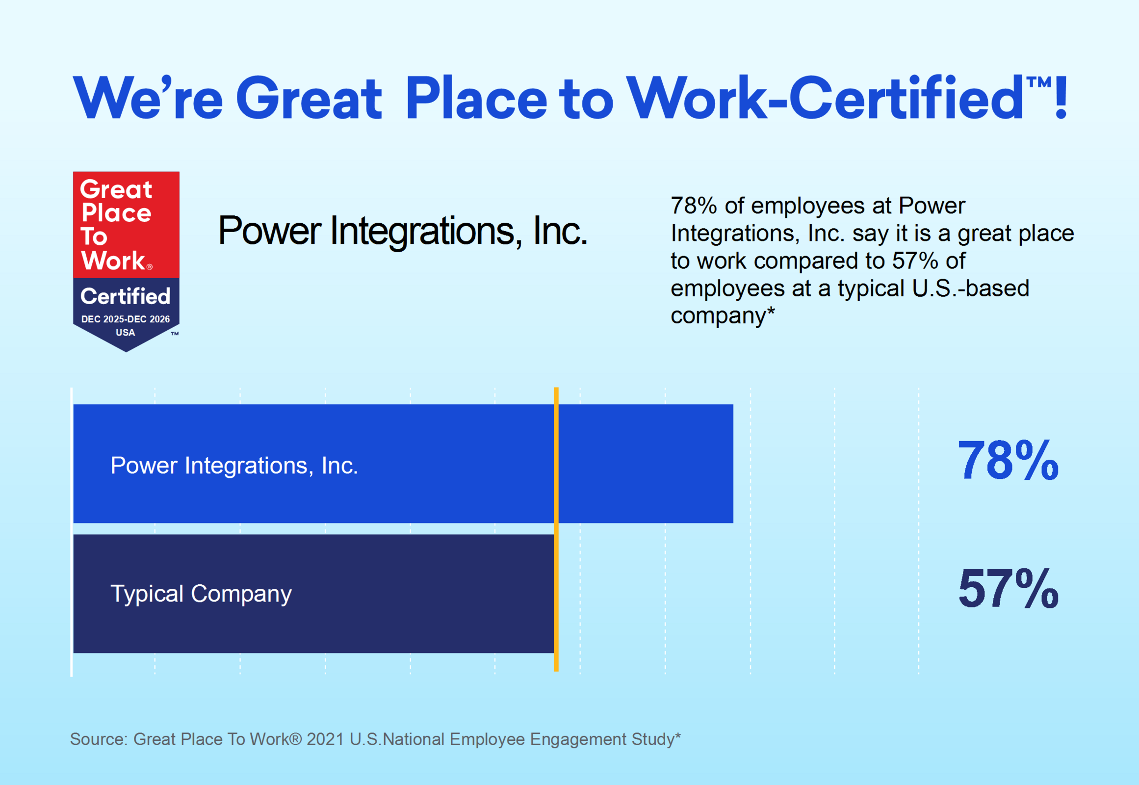
Innovation is the lifeblood of our company, and we depend on our people to sustain our competitive advantage. Power Integrations competes for the best talent. Our compensation packages consist of salary and equity, and they are commensurate with accomplishment.
It is the policy of Power Integrations to provide equal employment opportunity for all employment applicants and employees without regard to prohibited considerations of race, color, religion, sex (including pregnancy, gender identity and sexual orientation), national origin, age, disability or genetic information, marital status or any other classification protected by applicable local, state or federal laws.
Read the 2024 Sustainability Report >Applications Engineering
| Job listing | Job location |
|---|---|
| Apprentice Electronics Technician for Devices and Systems | Ense, Germany |
| Senior Hardware Design Engineer | San Jose, California |
| Senior System Power Supply Design Engineer (Data Center) | Pasig City, Philippines |
| Test Technician | Pasig City, Philippines |
Device Engineering
| Job listing | Job location |
|---|---|
| Senior Staff / Staff Engineer – GaN Technologist, Technology Development | San Jose, California |
Engineering
| Job listing | Job location |
|---|---|
| Principal Power System Engineer (Datacenter) | San Jose, California |
| Senior Power Systems Engineer (Datacenter) | San Jose, California |
| Senior Staff Power System Engineer (Datacenter) | San Jose, California |
| Sr. Staff Foundry Engineer | San Jose, California |
Finance
| Job listing | Job location |
|---|---|
| Accounting Operations Controller | San Jose, California |
| Senior Financial Analyst | Penang, Malaysia |
| Senior Financial Analyst | Penang, Malaysia |
Human Resources
| Job listing | Job location |
|---|---|
| Senior/Lead Talent Acquisition Partner - APAC | Pasig City, Philippines |
IC Design Engineering
| Job listing | Job location |
|---|---|
| Staff Digital IC Design Engineer | Cambridge, United Kingdom |
Information Technology
| Job listing | Job location |
|---|---|
| Oracle Financial Analyst | Penang, Malaysia |
| Sr. Techno-Functional Oracle Analyst, Supply Chain Management (SCM) | Penang, Malaysia |
Legal
| Job listing | Job location |
|---|---|
| Assistant General Counsel, Corporate | San Jose, California |
| Chief Intellectual Property Counsel | San Jose, California |
Operations
| Job listing | Job location |
|---|---|
| Foundry Planner | Penang, Malaysia |
| Procurement Specialist | San Jose, California |
Operations Engineering
| Job listing | Job location |
|---|---|
| Process Engineer | Ithaca, New York |
Package Engineering
| Job listing | Job location |
|---|---|
| Senior Packaging Engineer | Ipoh, Malaysia |
| Staff Package Engineer | Penang, Malaysia |
| Staff Packaging Engineer | Penang, Malaysia |
Product Development
| Job listing | Job location |
|---|---|
| PLM Change Analyst | Penang, Malaysia |
Product Engineering
| Job listing | Job location |
|---|---|
| Product Engineer | Penang, Malaysia |
| Senior Product Engineer | Penang, Malaysia |
| Staff NPI Product Engineer | Penang, Malaysia |
Quality Assurance
| Job listing | Job location |
|---|---|
| Failure Analysis Engineer | San Jose, California |
| Senior Field Quality Engineer | |
| Sr. Staff Reliability Engineer | San Jose, California |
| Staff Failure Analysis Engineer | Penang, Malaysia |
| Staff Failure Analysis Engineer IC | Penang, Malaysia |
| VP of Global Product & Quality Excellence | San Jose, California |
Sales
| Job listing | Job location |
|---|---|
| Account Manager | Taipei, Taiwan (Province of China) |
| Customer Service Representative | Penang, Malaysia |
| Customer Service Supervisor | Penang, Malaysia |
| Field Applications Engineer | San Jose, California |
| Field Applications Engineer | Munich, Germany |
| Key Account Manager | San Jose, California |
| Senior Field Applications Engineer | Shanghai, China |
Technology Development
| Job listing | Job location |
|---|---|
| Device Modeling Engineer | San Jose, California |
| Staff Device Engineer | San Jose, California |
Test Engineering
| Job listing | Job location |
|---|---|
| Senior Test Engineer | Ipoh, Malaysia |
| Senior Test Engineer | Penang, Malaysia |
| Sr. Staff Test Engineer | Penang, Malaysia |
| Test Development Engineer | Penang, Malaysia |
| Test Engineer | Ipoh, Malaysia |
If you don't see a role that fits your profile, then apply with our General Application.
Check on an application you've submitted.
Sign up for Job Alerts.